23
$\begingroup$

After the uncontested absorption of Hong Kong in 2020, China reasserted control over Formosa in 2022. In 2023 the Korean government reopened its war against its southern rebels, leading to their surrender in 2024. Despite prognostications of world war, these went largely without retaliation. Most of the Pacific nations signed treaties assuring their neutrality, and China turned its attention eastward.

Nonetheless, there was a notable casualty in the brief but bitter conflict. Many of the largest semiconductor fabrication plants, such as TSMC and Samsung, were in the rebel-held areas. During the fighting, the leaders of those areas identified them as too valuable to fall into enemy hands and a military and surveillance threat to future resistance. They were therefore targeted with military weapons - and clean rooms proved quite vulnerable to artillery fire. In the aftermath, China blamed the U.S. for supporting these attacks. A cold war of hacking, fires, sabotage, even "anonymous drones" ('UFOs') followed, in which plants in Dallas and Shanghai were largely incapacitated.

Major users of the chips were not entirely unprepared. Western commercial interests supported the Bitcoin Bubble as a cover for panic buying of chips in advance of the conflicts. Automakers and others began to reconsider the use of computing technology where possible. "Reduce, reuse, recycle" became the motto of industries with semiconductor exposure.

The initial, obvious solution was simply to build more plants, with \$37 billion earmarked for expansion in the U.S. alone by 2021. But with conflicts continuing to decrease production capacity, and disasters befalling producers even in Japan, this became a very hard sell. Who would invest $10 billion in a plant that could be destroyed in a few hours by inexpensive means?

The military of each country took matters into its own hands, producing chips in secret, hardened underground bunkers. But these were not designed with consumer products in mind - they were generally at a lower scale, radiation-hardened, and even when offered on the civilian market, contained "back doors" that spooked an audience that had already started, perforce, to put the Computer Age and its pall of paranoia behind them.

Your task is to propose the best new consumer computer manufacturing industry you can, with all the knowledge available today, provided it does not rely on external foundries or investments of more than ten million dollars before beginning production. (You can assume several years and billions of dollars of solid R&D funding could have happened in each country between 2021 and 2025, as long as it is not invested in one place or building a specific production plant.) The technology does not have to be the same as what is in use now! If you can pull out something with microfluidics, aerographene networks, quantum computing via NMR of large organic chemicals ... etcetera ... that's much more fun! But low-tech human-scale solutions are probably best for the plot.

$\endgroup$
3
  • $\begingroup$ Comments are not for extended discussion; this conversation has been moved to chat. $\endgroup$
    – L.Dutch
    Commented Mar 20, 2021 at 16:59
  • $\begingroup$ Who says? Why not write it, instead of asking us top write it for you? $\endgroup$ Commented Mar 20, 2021 at 18:43
  • $\begingroup$ Why is it hard to see that your, not our task is to propose the best new (anything)? Who but you might suggest the technology had to be what is in use now? If you want to work with microfluidics, aerographene networks, quantum computing via NMR of large organic chemicals, etc, go ahead: write it! If not, what are you Asking about? $\endgroup$ Commented Mar 20, 2021 at 23:33

11 Answers 11

19
$\begingroup$

Much Smaller Wafers and Much Larger Chips

Smaller wafers require smaller foundries, which should be more survivable. This will drive the foundries to older tech, so the transistors will be larger.

Process

In a nutshell, chip manufacturing is "Build a silicon wafer, put the wafer through a bunch of highly specialized machinery."

All this machinery must exist in a clean room, because static, dust, etc. will damage the end product. The high cost of building a foundry is partly a function of the high precision of those machines, and partly a function of building and maintaining a clean room.

The Change

So instead of starting with a wafer the size of a serving plate (12 inch diameter) go back to the "good old days" of the 1960s, and start with a 1 inch diameter wafer.

Now you get to scale down all of the other equipment!

The size of your clean room should go way down, which should make it much cheaper to build and maintain. Thus the investment is less, and the destruction of your factory is less catastrophic.

A smaller foundry should also be easier to protect - it's easier to bury, easier to monitor the perimeter, etc.

But won't you need more Foundries?

Yes.

But that's OK - instead of building a few, very expensive photoliography setups, you build lots of cheap ones. Build factories to build your chip factories.

Sure, you won't be able to keep the quality up - that's why you go with larger transistors, because the precision requirements are lower.

End Result

You'd probably end up with more expensive, less powerful chips, but you could have dozens of foundries spread across the country, each one churning out a relatively low volume of product.

$\endgroup$
11
  • 3
    $\begingroup$ "Crowdsource" the specialized part by lowering the requirements to "easier" (relative to the previous state) levels. :) Nice solution :) Plus it decentralizes the whole process. You must bomb out the whole nation to get all the factories and you'll just die trying. $\endgroup$
    – mishan
    Commented Mar 19, 2021 at 15:33
  • 4
    $\begingroup$ +1, but silicon and silicone (polysiloxane) are quite different materials. $\endgroup$ Commented Mar 19, 2021 at 19:02
  • 2
    $\begingroup$ @WaterMolecule - noted. $\endgroup$
    – codeMonkey
    Commented Mar 19, 2021 at 20:01
  • 6
    $\begingroup$ I dont see why smaller wafers means older tech and larger transistors. You can make a high resolution stepper for a small wafer. In grad school I processed 1 cm substrates by hand with features as small as 10 nm on a ~$1Million lithography tool. The whole lab cost only a few million and could do most of a cmos process. $\endgroup$
    – Matt
    Commented Mar 19, 2021 at 22:25
  • 4
    $\begingroup$ Matt and V. Sim are correct; major research universities can have small on-site fabs with 1-2 generation old processes that fit in one floor of a small building. see quora.com/…. This answer is at best only partially valid. $\endgroup$ Commented Mar 20, 2021 at 16:12
14
$\begingroup$

I imagine you'd see a return to the computers of the 1960s and 1970s built of discrete logic chips (TTL at the time).

If you still have access to modern manufacturing at the PCB and simple component level, something in the vein of retro-hobby projects like the MOnSter 6502 and the Gigatron, which reimplement a CPU using only logic chips.

(ie. chip designs from before VLSI that are just the 1960s-state-of-the-art way to pack 3 or 4 transistors into a smaller, easier-to-wire package.)

The Gigatron kit does use a RAM chip and a ROM chip, but those can be built using transistors and diodes. (and capacitors if you want dynamic RAM) They're just significantly more bulky and, since it's a hobby kit focused on making a CPU without a microprocessor, it'd be counter-productive for the Gigatron to do that.

(See Visualizing ROMs 1: Diode Matrix ROM (Hackaday) for more on building ROM from scratch.)

...and I do hope you do have access to things like surface-mount transistors and pick-and-place machines or it's guaranteed to be cost-prohibitive as a consumer product. Even the Apple 1 used the kinds of complex ICs you're trying to avoid and it was pretty pricey after inflation despite how minimal it was. In this day and age, we take for granted how high the base cost of stored-program computing is.

$\endgroup$
5
  • 1
    $\begingroup$ This is the correct answer. You will eventually need integrated circuits; no need to pursue the dead paths of mechanical, relays, or vacuum tubes. Start with small-scale integration, and iteratively build chips at larger scales. $\endgroup$
    – DrSheldon
    Commented Mar 20, 2021 at 0:02
  • $\begingroup$ TTL seems like a great way to accelerate the climate crisis. $\endgroup$ Commented Mar 21, 2021 at 16:42
  • $\begingroup$ @R..GitHubSTOPHELPINGICE Any regression in technology will accelerate the climate crisis. Even switching to a pre-industrial lifestyle without prompting mass starvation might do so, given the tendency to clear rainforest for farming by burning it. $\endgroup$
    – ssokolow
    Commented Mar 21, 2021 at 19:18
  • $\begingroup$ I still can't imagine doing TTL when you know how to do CMOS. Even with discrete components you should be able to do CMOS logic. $\endgroup$ Commented Mar 21, 2021 at 20:16
  • $\begingroup$ @R..GitHubSTOPHELPINGICE I was more referring to how, in the era when things like the PDP-11 were still being built out of massive amounts of discrete logic, TTL was the technology used. "Refrigerator-sized thing made out of discrete logic" was the key part and "last time we did that, we were using TTL" was secondary. (EDIT: There. I've de-emphasized the TTL part.) $\endgroup$
    – ssokolow
    Commented Mar 21, 2021 at 22:42
7
$\begingroup$

Assuming that you want computing in the numerical sense, and don't require electronics, then you can do many things with clockwork. Wikipedia gives a better summary than I can.

For the general-purpose "computer" of today, you're likely to run into the same problems as Turing, Lovelace, and Babbage - too many parts.

$\endgroup$
7
$\begingroup$

There are alternative technologies and, now, a strong drive to invest on them

If a main technology becomes unfeasible or too costly, then alternative technologies will become more competitive and attract more money and resources (which otherwise would be invested in the main technology).

For instance, Organic electronics allows to create circuit from printing plastics.
Obviously, ther peformance of such devices is a lot worse than semiconductor electronics, but after the destruction of silicon foundries, they will attract a lot more investments than they would if semiconductors were still feasible.
After some time, organic electronics will probably not close the gap with semiconductor electronics, but will surely improve enough to be employable for computers.
Probably such computers will be bulkier than our computers, but for instance they could architecturally employ some of the pros of organic electronics (eg. the lower cost), for instance focusing even more on parallel processing in order to improve their performance.

$\endgroup$
1
  • 2
    $\begingroup$ Would organic electronics be subject to its own "Moore's Law" starting from scratch, possibly with a different exponential rate constant, or could it leap to the present semiconductor Moore's Law, or something else? this seems optimistic about its relevance even in a normal market, but I have no idea how believable it is. $\endgroup$ Commented Mar 19, 2021 at 17:10
5
$\begingroup$

not rely on external foundries or investments of more than ten million dollars before beginning production.

Best I can do is this:

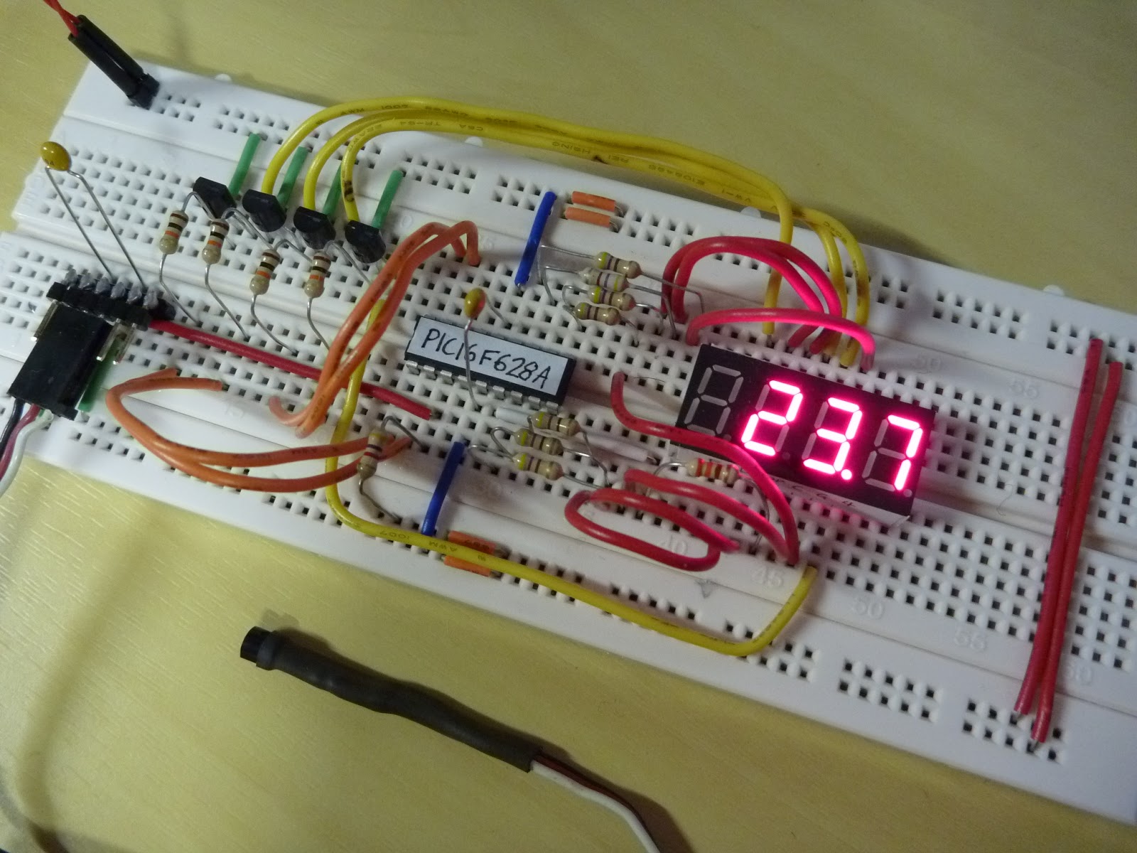
A breadboard with some parts soldered into it

Anything requiring the finesse of even 80's level electronics will require more than a couple handful million dollars nowadays. Breadboards on the other hand can be assembled from trash, and you can throw in some cheap LED's and resistors on top of it to do some computing.

Sure, a simple calculator will weight a handful hundreds of grams and will be as fast as a snail... But hey, on that budget, it's this or going back to the abacus.

$\endgroup$
3
  • 20
    $\begingroup$ The breadboard is a bit of a red herring - you could do the wiring with a soldering iron and a piece of cardboard, I think. But where does the PIC16F628A come from? How much investment is required to make those? $\endgroup$ Commented Mar 19, 2021 at 1:34
  • 3
    $\begingroup$ @MikeSerfas it's a post apocalypse scenario, you scavenge for those. $\endgroup$ Commented Mar 19, 2021 at 13:31
  • 5
    $\begingroup$ "Cheap LEDs" wouldn't be a thing either if all the semi-conductor plants have been obliterated. Diodes (including LEDs) are basically just 2 semi-conductors in a casing. Sure we have a lot of them lying around now, but those would get used up fast if the supply stopped coming in. $\endgroup$ Commented Mar 19, 2021 at 13:50
5
$\begingroup$

3D Printing Integrated Circuits

We can already 3D print PCBs. There are multiple companies working on 3D printing semiconductors.

By nature, 3D printers are slower than dedicated manufacturers for the same volume, but an individual 3D printer is often cheaper and more mobile than the smallest reasonable dedicated manufacturing plant.

Instead of huge manufacturing plants, you can set up mobile manufacturing trucks that set up in a dedicated location and then leave if things look like they might get messy. Since a bunch of 3D printers on the back of a semi truck is likely to produce chips cheaper than the government's super secret underground laboratories, they will likely provide you with advance warning of bombing runs aimed at locations near your trucks so that they can move vital equipment and personnel.

Eventually, someone will release these 3D printers to the consumer market, decentralizing production to the point where it would be impossible for foreign powers to bomb them.

Obviously, you're probably looking at more expensive computers that are less powerful for a few decades, but eventually some mega-corporation will spend a few hundred billion dollars on secret bunkers that make the US government's cry, and everything will normalize.

$\endgroup$
2
  • 2
    $\begingroup$ 3D printers with nanometer-scale pins? Yeah, right. Yeah, right???! This looks like a promising direction, if it's true... $\endgroup$ Commented Mar 19, 2021 at 17:14
  • 1
    $\begingroup$ That was almost exactly my reaction when I read about it $\endgroup$
    – SirTain
    Commented Mar 19, 2021 at 17:39
4
$\begingroup$

Believe it or not, there is actually such a thing as amateur semiconductor manufacturing.

A fellow on YouTube by the name of Sam Zeloof has made his own integrated circuits and covered the process in detail, including a clever adaptation of a DLP projector for maskless photolithography. I think he said the feature size he can get is around 10 micrometres. That's what Intel used to make the 4004 back in 1971.

It's not a fast process, but it can be done at a small scale at home with the equivalent of a garage full of equipment.

You could rebuild the semiconductor industry in a decentralised fashion. If anyone with a few thousand dollars for equipment and a garage to put it in can get into chip manufacture, then you could have thousands of small outfits making chips and spreading things out so much it's no longer practical to try and take them all out.

Now, I'm sure that at first it wouldn't be too much better than what Sam is pulling off now, but give it a few years with companies specialising in making home-fab equipment and you could get into 486-level stuff (800nm) at home. Just look at how 3D printers have developed over the last decade.

Chip-fabbing could be the new 3D Printing. Some people doing it as a hobby, others building a small business around it. A small city might have three or four fab-on-demand businesses to supply chips needed to repair stuff. Hell, you could probably find quite a few people who design chips as a hobby and leave the actual fabbing to one of their local fab-on-demand companies because they're just not interested in that side of things.

Oh, and don't forget the impact of open source stuff here. You'd probably have thousands of chip designs available for download. Some might be replicas of old chips that have been reverse-engineered (eg. custom video chips from old computers or games consoles), others could be completely new designs for various uses. We kind-of have something along these lines already, but rather than being designs to etch into silicon with photolithography, they're a bit more abstract and written in languages like Verilog and VHDL, and after a translation process analogous to compiling software, usually get used to configure an FPGA, rather than making fixed-function silicon chips.

$\endgroup$
3
$\begingroup$

Frame challenge

You put the foundries underground.

10 meters of earth are surprisingly difficult to destroy.
10 meters of stone (even soft stone), and you need military-grade weaponry to even make a dent into them.

Ventilation and such will be a challenge, but again: If you invest billions, a few millions for good airflow won't change the budget much.

Usually you don't even need that. A wire fence, a dirt wall and/or cheap buildings around the expensive/dangerous parts of the facility to prevent RPM attacks, and access control are what industrial

Going underground is the standard solution for cheap hardening against attacks if you don't have to be mobile. This holds even for high-tech military forces, and since the assumption is that the attacks are cheap, 10 meters of dirt and a guarded gate will prevent that.
(All oil facilities should have something like that. Particularly in conflict regions like Nigeria, Syria or Iraq. None of these even went underground - of course it's merely millions that blow up, not billions, so billion-dollar facilities would have roughly 1000 times the attractiveness to attackers - but also 1000 times the budget for better protection.)

Real-world examples

Any industrial facility is actually easy to destroy with bombs, particularly if the bombs are of the cruise missile variant.
So everybody who ever wanted a bomb-resilient facility put them underground: Ghaddafi's chemical plants, North Korea's nuclear facilities, Nazi weapons industry during WW2.
The Nazi example is particularly enlightening: They built these underground factories during the war, under daily and nightly bomb raids, and got them functional with little problems. (It didn't help them much, fortunately, because they were short on almost every raw material you can imagine: metal, oil, rubber.)

  • The foundries may not actually be the target

  • If the plans are somewhat more long-term, attack the equipment manufacturers. It's a damage multiplier, since you destroy the ability to build the next series of foundries.
    It's what we expect of the Chinese. Well, unless maybe in a heated war - then they'd follow short-term and long-term goals. (On the other hand, that's soo cliché. Plus maybe the story's circumstances don't allow long-term plans anyway.)

Let's see what fits inside the framing

The hypes of today won't make it:

  • Quantum computing, even if it became cheap (which won't happen before 2050 I'd say), is not a replacement for classic computing. We're roughly at the level of the Zuse machines with that: Sort-of works but it's still a looong way to go to make the technology a commodity. The next step would be software design: They're different enough that you need to invest new programming paradigms (like object-oriented or functional programming), and we needed roughly 20 years for each of these to make them sort-of work, and another 20 years to actually understand them.
  • Other switchable things like ferrofluids and whatnot will be as expensive as silicon to produce: Today's silicon industry is expensive because you need ridiculous purities for the wafer silicon, and ridiculous manufacturing precision (sub-wavelength!); any alternate technology will suffer from the same problem.

** Things that would work inside the framing**

  • Recycling - you'll get a specialist industry but it's workable. Lots of people who will promise but just burn the reballed CPU, so workmanship will be a big topic. The problem is that you need the right chips - you can't combine all chips, so everybody who's doing the recycling will have large chip stores, and some system to find the chips that they stored three years ago. (The stores are still attackable targes, and small stores are far less useful than large ones. Plus you will need facilities for making PCBs - modern chips require multi-layer PCBs, that's not easy to manufacture either.)
    Now recycling still isn't very sustainable. There's going to be growing scarcity - some people will hide the despair with activity, others will openly despair, yet others will operated on the premise "we have problems but so has the enemy, and we don't need to have IT, our IT just needs to fail later than theirs". (That might be a pretty interesting plot point, and it's very easy to show instead of tell it.)
  • Human calculators, accountants. You know, these were a thing before we had electronic computers.
    In a recycling scenario, these will become more and more important. There were specialists for calculating logarithms, specialists for calculating ballistic curves, specialists for adjusting machines, so the world will be gradually shifting towards these. These have the advantage that they're easier to "program" than machines: You just tell them, train a bit, and if there's an error, you will be able to understand why and how to fix it.
$\endgroup$
2
$\begingroup$

To begin with, besides a guy who DIY chips in a garage First IC :) – Sam Zeloof, on techprocesses of 70's, there is another valuable resource The Chip History Center - The Virtual Museum of Semiconductors

So as mentioned in the comments The MOnSter 6502 a disintegrated version of actually MOS Technology 6502 chip and reading through the history of actual chip and clicking links in it that yields some results.

Not a surprise that the mid-'70s was somewhat a turning point for the chips production prices and consumer-grade solutions. And that turning point was the projection of the mask instead of it necessarily touching the wafer.

Equipment that did the change was Micralign - it improved the life of a mask by 4 orders of magnitude from 10 to 100'000 and reduced mask-induced defects 5-6 times for chips of that time.

Micralign 100 The first sale of what was now known as the Micralign 100 was in 1974 to Texas Instruments, which paid \$98,000 for the machine, equivalent to \$508,053 in 2019, about three times that of existing high-end contact aligners.[19] Sales to Intel and Raytheon followed. Intel kept their system secret, and were able to introduce new products, notably memory devices, at prices no one else could touch. The secret finally leaked out when various Intel workers left the company.

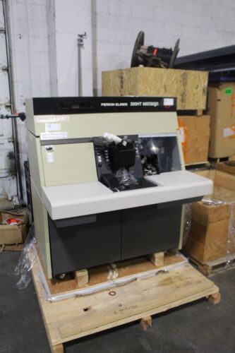
What looks like a more modern version of the Micralign 100, an Perkin-Elmer 300HT Micralign Mask Aligner, which can be googled and a lot of places and offers can be seen on those, used their price seems to be around \$15'000, there is some offers on ebay for 2 grand, so it seems depends on conditions and such. So as what seems to be more modern versions and with lesser working hours around $55k

How the thing looks like:

Perkin-Elmer 300HT Micralign Mask Aligner

It is good for 4" wafer size, the other specs are it seems to be good for 1.25um tech processes.

There is quite a lot of those in circulations and they are part of lab equipment as of today, old equipment. A foot print around 1.7 square meters and I would say it is compact.

This sort of equipment is just part of the chain, but never the less an important one and what actually help you to "draw" the schematics on a wafer.

Applying photoresists and heat ovens and etching - those also require equipment, so making masks requires equipment.

But from the looks of it, you can land on somewhat early or mid 80's specs with \$10kk with used equipment or maybe new.

if you scavenge for modern guts/brains for them, modern piezoelectric actuators - I guess those can be drastically improved in terms of the making of those, with technological capacities which are available today. As if replicating their old days manufacturing methods may lead to other expenses.

So it is hard to tell what it may cost to produce a new unit, be it its modernized version or as in the good old days. But overall it does look like it is not impossible to be on the budget you propose for a single production node, full cycle.

This kind of equipment requires a lot of manual work, this page contains how intel fab processes looked like in 80's: An Intel Wafer Fab Cleanroom Circa 1980 - for me it looks like a somewhat typical biological laboratory, meaning it does not look totally insane so as it already looks like they are under the ground, lol.

so it may have a good touch of a modern redesign for our current production paradigm, along the general modernization, but that R&D will be smeared over all those factories you build, so...

Overall, some useful keywords are: Micralign, Stepper

Results are on pair with 80's, and at least it somewhat shows that if someone throws few billions in it, it definitely can be done better than just 80's, producing relatively compact nodes of production, and 80's are the low bar.

$\endgroup$
1
$\begingroup$

Farms, not plants.

genetically engineered cow

There is already great interest in biological synthesis of semiconductor components. Semiconductor foundries are large and delicate. Life forms routinely undertake operations of comparable delicacy.

https://spectrum.ieee.org/semiconductors/materials/germs-that-build-circuits

By the time you read this, there's a good chance a virus has built a transistor. Last July.. Angela Belcher make a bold prediction: within six months, her laboratory... would have genetically engineered a virus to coat itself in a crystalline semiconductor sheath and locate and bridge two electrodes--thus forming the critical part of a field-effect transistor, the kind on which most computer chips rely. If Belcher delivers, it will dramatically illustrate biology's promise in furthering nanotechnology, the manufacture of circuits and devices only billionths of a meter in size.

Biological self-assembly, as this field of research is called, has a compelling appeal. Living creatures produce the most complex molecular structures known to science. Crafted over eons by natural selection, these three-dimensional arrangements of atoms manifest a precision and fidelity, not to mention a minuteness, far beyond the capabilities of current technology.... In projects now under way, scientists are using proteins and DNA, the molecule that encodes genetic data, to construct nanometer-scale crystals of semiconductor atom by atom, bind to precious metals, distinguish between different nanoparticles by their electrical properties, and otherwise choreograph the arrangement of nanoscale components.

... The Army and others see a role for biological self-assembly in fabricating future sensors, displays, and magnetic storage devices, as well as in energy production and information processing.

In this near future, political instability accelerates the development of organic semiconductors synthesized by organisms.

At the same time, the advent of CRISPR gene manipulation produces a revolution in drug development. Many drugs once produced in giant bioreactors can instead be produced by farm animals and excreted in milk. The animals are normal animals and the milk normal milk. The milk is processed to extract the drugs. Genetically engineered animals producing drugs is no longer fiction.

https://www.theverge.com/2016/12/3/13819482/genetically-engineered-animals-drugs-sab-cows-pharming-future

SAB’s cattle are just the latest example of lab-made animals engineered to be drug factories. Last year, the US Food and Drug Administration approved a genetically modified chicken that makes a drug in its eggs to treat "lysosomal acid lipase deficiency" — a rare genetic condition that prevents the body from breaking down fatty molecules inside cells. In 2014, the FDA approved a drug collected from the milk of lab-made rabbits to treat hereditary angioedema, a genetic disease that causes body swelling and can be fatal. And in 2009, the FDA approved a genetically altered goat that can make a drug in its milk that prevents fatal blood clots.

These transgenic animals are promising because they could make drug-manufacturing cheaper in the long run. Once created, the animals can basically keep pumping out drugs at a low cost — the cost of maintaining chickens and goats in a farm. And now that new gene-editing techniques like CRISPR-Cas9 are making swapping and inserting genes easier than ever, creating new animals in the lab will be faster and cheaper. “I expect that we will see this progressing at light speed now,” says William Muir, a professor of animal sciences at Purdue University. “We know the technology, we know how to use it, and we’re just waiting for, how many applications can we use it for?”

In your near future, organic semiconductors meet pharm animals and semiconductor synthesis moves outside. Engineered animals breed true and as a neat byprodct, the milk and eggs retain nutritional value and are still good for that after semiconductors have been processed out. The price of semiconductors falls dramatically. Semiconductor industries are no longer valuable targets.

$\endgroup$
2
  • 2
    $\begingroup$ Two criteria of a great answer: a) Absolutely lunatic b) Scientifically sourced. tthere is no guarantee that this technology, as promising as it is, will really lead to practical nanometer-scale devices." $\endgroup$ Commented Mar 20, 2021 at 17:00
  • 2
    $\begingroup$ ... This idea is more useful in a larger context. (Q: how was the main engine hacked? A: we missed it. Better A: it started when a flower grown aboard the ship produced surveillance cameras in its pollen.) $\endgroup$ Commented Mar 20, 2021 at 17:17
1
$\begingroup$

China is hostile? Intel doesn't care.

Look at the list of the semiconductor fabrication plants in the OP. In particular, look at Intel. Almost all of their plants are in the United States, and the ones that aren't are located in Western countries like Israel or Ireland. If China starts making chips from Taiwan and Japan non-viable in America, it won't hurt them. Heck, by knocking out so much of the competition, it might even help them!

The price of the raw materials might go up and hurt their bottom line a little bit, since China currently produces 79% of the world's elemental silicon, but the stuff is found basically everywhere so building facilities for mining and refining it should be entirely possible.

$\endgroup$
2
  • 1
    $\begingroup$ The OP's basically knocked out all of...five of the fabs in the Western world, which has about 120, with 2/3rds in the US and the other 1/3rd in Europe. They'd have to go on a coast-to-coast rampage to knock out the US fab capacity, and that still leaves European and Israeli fabs as well as some bits and bobs in other places as well -- I can imagine that ST would be going all-in on investment at this point given that their order book would be miles long and most of their fab capacity outside the Far East is in Europe $\endgroup$
    – Shalvenay
    Commented Mar 21, 2021 at 13:18
  • $\begingroup$ @Shalvenay "They'd have to go on a coast-to-coast rampage to knock out the US fab capacity" Yeah, the scenario in the OP doesn't really describe the sort of invasion of the continental US that would be required for China to knock out domestic industry. $\endgroup$
    – nick012000
    Commented Mar 21, 2021 at 13:28

You must log in to answer this question.

Not the answer you're looking for? Browse other questions tagged .